PCB assembly
In the realm of electronics manufacturing, Printed Circuit Boards (PCBs) play a crucial role, serving as the foundation upon which electronic components are mounted and connected. PCB assembly, therefore, stands as a pivotal process in the creation of electronic devices, facilitating the integration of various components onto the board to bring a design to life.
At its core, PCB assembly refers to the process of populating a bare PCB with electronic components such as resistors, capacitors, integrated circuits, and connectors. This intricate procedure involves several stages, each meticulously executed to ensure the functionality and reliability of the final product.
The journey of pcb assembly typically begins with the fabrication of the bare PCB. This involves etching a pattern onto a copper-clad substrate to create conductive pathways, known as traces, that will form the electrical connections between components. Once the bare PCB is manufactured, the assembly process can commence.
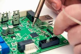
What is PCB assembly?
The first step in PCB assembly is the application of solder paste onto the board. Solder paste, a mixture of tiny solder particles and flux, is precisely deposited onto the PCB using a stencil. This paste serves as the adhesive that will hold the components in place during the subsequent soldering process.
Following the application of solder paste, the components are placed onto their designated positions on the PCB. This step, often performed by automated pick-and-place machines, requires precision and accuracy to ensure proper alignment and orientation of each component.
Once all components are in place, the PCB undergoes a process called reflow soldering. During reflow soldering, the entire assembly is subjected to controlled heat, causing the solder paste to melt and create secure electrical connections between the components and the PCB. This process is essential for achieving reliable electrical and mechanical bonds.
After reflow soldering, the assembled PCB undergoes inspection to detect any defects or inconsistencies. Automated optical inspection (AOI) systems are commonly employed to scan the board for issues such as missing components, misalignment, or soldering defects. Any discrepancies identified during inspection are rectified before proceeding to the next stage.
Upon successful inspection, the assembled PCB may undergo additional testing to verify its functionality and performance. Functional testing involves applying electrical signals to the board and observing its response to ensure that all components are working as intended. This rigorous testing phase helps identify any potential issues before the PCB is incorporated into the final product.
Once the assembled PCB passes all quality checks and tests, it is ready for integration into the electronic device it was designed for. Whether it’s a smartphone, a computer, a medical device, or an automotive component, the PCB serves as the central nervous system that enables the device to function.
In conclusion, PCB assembly is a complex yet essential process in electronics manufacturing, responsible for bringing electronic designs from concept to reality. From the meticulous placement of components to the precise soldering techniques employed, every step in the assembly process contributes to the creation of reliable and high-performance electronic devices. As technology continues to advance, the importance of PCB assembly in shaping the future of electronics cannot be overstated.