Stencils in PCB SMT Assembly
Stencils play a fundamental role in pcb smt assembly. They provide a precise template for depositing solder paste on the surface of a circuit board. The openings on a stencil correspond to the pads on the board, and an operator positions and secures the stencil in place using a frame before applying pressure to force the solder paste through its openings. This enables an accurate and consistent deposition of paste, reducing the likelihood of tombstoning, bridging, or other defects in the final PCB product.
The design of a stencil must be adapted to the type and size of components being assembled. For example, smaller packaged components require a thinner stencil than larger ones. The thickness of the stencil also depends on the space between individual components. For narrow spacing components, a thinner stencil is required to reduce the distance between each pin. For wide spacing components, a thicker stencil is used to accommodate the larger distance between individual pads.
Various techniques can be used to create the apertures in a stencil, including chemical etching and laser cutting. Both processes use subtractive methods to form the apertures, but the laser-cut process offers superior results as it does not leave rough edges on the aperture sidewalls. This is especially important because a smooth edge is necessary for the best solder paste release. Develop standardized repair procedures for common defects. Document each rework instance to track recurring issues and improve the assembly process.
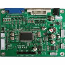
The Role of Stencils in PCB SMT Assembly
A metal stencil material is also important, and there are several choices. Stainless steel is the most common choice, offering durability and strength. Another popular option is aluminum, which is lighter and more cost-effective. However, it is less durable than stainless steel and can be prone to corrosion. Stencils can be made from polymer or plastic as well, but these materials offer less accuracy and precision than metals.
To ensure that a stencil produces the desired results, it is important to make sure that it is flat after being laser cut or etched. A non-flat stencil will cause misalignment during printing and can lead to poor gasketing, resulting in inconsistent paste application and other defects on the finished PCB. Datum’s production methods help to eliminate these problems by ensuring that the stencil is extremely flat after etching or laser cutting.
Once the stencil is in place, an operator aligns it to the pads on the pcb smt assembly and applies solder paste, a mixture of copper and solder alloy. Then, the operator uses a squeegee to apply pressure to the stencil, forcing the solder paste through its openings. The squeegee is then removed, and the deposited paste is inspected for defects before moving on to the next step in the manufacturing process. The squeegee can be cleaned with an approved solvent to remove any residual solder paste, and the stencil should be stored in a protective case or cover when not in use to prevent damage. This will also extend the lifespan of the stencil and preserve its accuracy and precision.