4 Layer PCB Board Can Handle
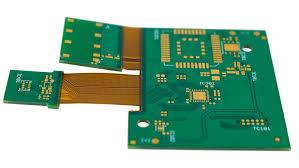
The maximum current a 4 layer pcb board can handle depends on the design of its power and signal circuits. The circuits should have a sufficient current capacity to meet the demands of the application without exceeding the design limits. The power and signal paths should also be properly routed to minimize the impact of noise on the circuits.
There are several techniques that can be applied to the power and signal layers of a PCB to increase its current carrying capabilities. These include widening the traces, increasing their copper thickness and adding internal plane layers. These measures can significantly improve the current carrying ability of a PCB.
Another method of improving the current capacity of a PCB is to use a separate ground plane. This can help to reduce the parasitic capacitance and inductance of the signal layers, and will also allow for higher currents to be drawn through them without increasing the voltage drop. It is important to keep in mind that the ground plane should be well connected to the power supply pins, and there should be no gaps in the connection.
It is also important to use multiple ground planes, as they can act as shields for the inner signal layers. This will help to prevent unwanted crosstalk and electromagnetic interference (EMI), especially when high-speed signals are routing between the signal layers. Using multiple ground planes will also lower the ground (reference) impedance of the PCB, and this will minimize the common-mode radiation that can cause interference problems.
Maximum Current a 4 Layer PCB Board Can Handle
When designing a PCB that will be used for high-current applications, it is crucial to size the conductors appropriately. This will ensure that the temperature rise of the conductors stays within a safe limit for the required operating current.
One useful tool for this is the IPC 2152 nomograph, which is a graph that shows the maximum recommended conductor width for a specific current. The nomograph provides a quick and easy way to determine the maximum current that a particular power or signal trace can carry, and it can be easily adjusted for different copper weights and laminate materials.
In addition to the above-mentioned techniques, it is essential to make sure that the layers of the PCB are matched in terms of their coefficients of thermal expansion (CTE). This will prevent misalignment and offset vias due to differential CTE between the different materials used in the construction of the layers of the PCB. This will help to avoid unnecessary stresses and cracks in the material during manufacturing, which can lead to failure of the circuit. By following the above guidelines, engineers can design a high-current PCB that will be able to withstand substantial amounts of current.
This can be crucial in applications such as LED drivers, battery systems, motor controllers and other high-power electronic devices. By mastering these techniques, electrical engineers can produce reliable, optimized PCBs that are capable of handling substantial currents. The demand for current capacity in modern electronics keeps growing, and mastering these methods can allow designers to meet the needs of these applications.