Create a Via in Pad
In circuit board design, a via is a plated hole that helps link copper traces from one layer of the PCB to subsequent layers. High-density multi-layer boards can use blind vias that are visible only on one surface or buried vias that are not visible at all. Both types of vias are useful in connecting signal lines between pads and devices on the PCB.
Vias are often used in circuit boards, but they can also create problems when they are not designed properly. In particular, they can increase parasitic inductance and affect the signal integrity of high-speed nets. In order to minimize these effects, designers can choose to use a technique called via in pad (VIP). This is where the via is inserted directly into the pad rather than drilled through the entire PCB.
There are many benefits of using VIP in your PCB. The primary advantage is that it allows for more efficient routing of signals. Specifically, it can help to reduce the length of the signal path and reduce inductance. This can be particularly beneficial for high speed designs and interfaces.
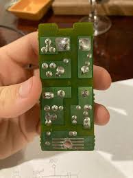
How to Create a Via in Pad
Another benefit is that it can improve signal quality. By reducing the inductance of the signal path, it can allow for faster speeds and lower noise. Additionally, it can also improve the mechanical reliability of the connection by reducing the stress on the pad.
One downside of using VIP is that it can introduce additional steps to the manufacturing process. Unlike traditional vias, which are drilled with a mechanical drill and go all the way through the board, via in pads require that the contract PCB manufacturer cap the via with a conductive epoxy and then plate over it with copper. This extra step can add time to the manufacturing process and cost more.
In addition, the via-in-pad must be carefully designed to avoid manufacturability issues. For example, if the pad is too close to the via, it may cause shorting during soldering. It is important to ensure that there is sufficient clearance between the pad and the via cap to prevent this from happening. It is also important to ensure that the pad size, shape, and relief meet manufacturability requirements.
Finally, it is essential to ensure that the via in the pad is adequately filled and plated to withstand thermal cycling and mechanical stress. Insufficient filling or plating can lead to solder wicking during assembly, which can cause the via and pad connection to fail due to insufficient solder. Therefore, it is important to specify the proper filling and plating options for the PCB manufacturing process and to run detailed design for manufacturing checks (DFM) on the via in pad layout to ensure that all of these factors are taken into account. Close communication with the contract PCB manufacturing company can also help to avoid these types of errors.