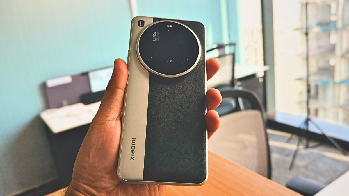
HDI Printed Circuit Boards
The use of hdi printed circuit boards is growing in popularity for various applications in electronic devices. From mobile cellular phones and touch-screen devices to high-performance digital cameras, 5G network communications and military equipment such as avionics and smart munitions. This new technology offers improved PCB signal integrity using a smaller board footprint.
The key advantage of HDI is its lower overall manufacturing cost. Its thinner dielectrics allow for a lower component and board thickness, thus significantly reducing materials costs. It also reduces power consumption, as less energy is needed to transmit signals between components. The small board size also allows for greater functionality and value out of a single PCB that would require multiple traditional boards to meet the same performance standards.
Moreover, hdi printed circuit boards can be made with thinner dielectrics to reduce the risk of signal reflection and radiation. The smaller via sizes improve the electrical performance of the board, as they can handle higher frequencies with reduced signal losses and crossing delays. The smaller vias also reduce parasitic capacitance and inductance that can cause noise coupling and EMI issues. Furthermore, the elimination of dog-bone pads and the use of filled plated microvias that connect directly to component solder lands further reduce inductance in the distribution network.
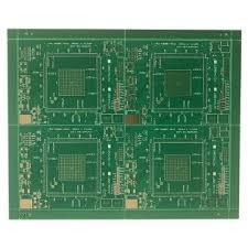
How HDI Printed Circuit Boards Can Be Used in RF Applications
As a result, HDI circuits can provide more reliable performance in demanding applications. In addition to lowering the cost of production, HDI PCBs can also be made in shorter lead times. This means that the product you need can be in the hands of your customers much faster.
Another benefit of HDI PCBs is their ability to accommodate a wider range of technologies, such as 3D printing. This new process enables designers to create intricate geometries that would be impossible with traditional methods. This opens up a whole new world of possibilities in electronics design.
While there are many benefits to hdi printed circuit boards, you should be aware that these boards can be more challenging to design. You will need to take into account the different fabrication processes and limitations when designing your layout. This will affect the via size and the number of layers you can use. You should always check with your manufacturer to determine the limits of their fabrication capabilities. This will influence the maximum ball pitch that can be used on your BGA components and the number of layers you need to route all signals. You can use the layer count calculator in your routing tool to help you determine this.