custom pcb manufactured
Custom printed circuit boards (PCBs) are essential components in the electronics industry, serving as the foundation for countless electronic devices. The manufacturing process for custom PCBs is a complex and precise procedure that involves several steps, each crucial for ensuring the quality, reliability, and functionality of the final product. Here’s an overview of how custom PCBs are manufactured:
The manufacturing process begins with the design and layout of the custom pcb. Designers use computer-aided design (CAD) software to create the PCB layout, specifying the placement of components, routing of traces, and other design parameters. During this phase, designers optimize the layout for electrical performance, signal integrity, thermal management, and mechanical considerations.
Once the design is finalized, the next step is selecting the appropriate materials for the PCB. The choice of materials depends on factors such as the desired electrical properties, thermal characteristics, mechanical strength, and cost considerations. Common materials used in PCB manufacturing include fiberglass-reinforced epoxy laminate (FR-4), aluminum, ceramic, and polyimide.
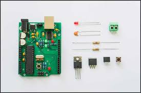
How are custom pcb manufactured?
The selected substrate material, typically a thin sheet of fiberglass or other laminate material, undergoes preparation before the circuitry is applied. This may involve cutting the substrate into the desired size and shape, cleaning the surface to remove any contaminants, and applying a thin layer of copper foil to one or both sides of the substrate.
The next step is to print the circuitry onto the substrate using a process called etching. A photoresist material is applied to the copper foil, and the PCB layout is transferred onto the photoresist using a photographic mask or stencil. The PCB is then exposed to ultraviolet light, which hardens the photoresist in areas where the circuitry is to be retained. The unexposed areas are then washed away, leaving behind the desired circuit pattern.
After the photoresist has been developed, the PCB undergoes etching to remove the excess copper foil and reveal the circuit traces. The PCB is immersed in an etching solution, typically containing chemicals such as ferric chloride or ammonium persulfate, which selectively dissolve the unprotected copper. Once the etching process is complete, the remaining photoresist is stripped away, leaving behind the finished circuitry.
Holes are drilled into the PCB to accommodate through-hole components and vias. High-speed precision drilling machines are used to accurately drill holes of varying diameters and depths according to the PCB design specifications. These holes provide electrical connections between different layers of the PCB and allow components to be mounted securely.
Once the PCB has been drilled, the next step is to place the components onto the board. Surface-mount components are typically soldered onto the PCB using automated pick-and-place machines, which precisely position the components onto the solder pads. Through-hole components are inserted into the drilled holes manually or using automated insertion equipment.
The final step in the manufacturing process is soldering, which forms the electrical connections between the components and the PCB traces. There are two main methods of soldering: wave soldering and reflow soldering. Wave soldering is used for through-hole components, where the PCB is passed over a wave of molten solder that coats the exposed metal surfaces. Reflow soldering is used for surface-mount components, where solder paste is applied to the solder pads, and the PCB is heated in a reflow oven to melt the solder and form the connections.
After soldering, the PCB undergoes testing and inspection to ensure that it meets the required quality standards. Automated testing equipment checks for electrical continuity, shorts, opens, and other defects. Visual inspection is also performed to check for soldering defects, component misalignment, or other assembly issues. Any defects or anomalies are identified and corrected before the PCB is shipped to the customer.