Can printed board assembly be used
Printed circuit board assembly (PCBA) is the process of connecting all components of an electronic device in such a way that they function as one unit. This involves integrating all the essential functions and components like resistors, diodes, integrated circuits, capacitors, and more. These are then soldered together to create the final product, such as a computer, tablet, or mobile phone.
A good printed board assembly is essential to ensure that a device performs as designed. While there are several ways to assemble a PCB, two of the most common methods are Surface Mount Technology (SMT) and Through-Hole Technology (THT). However, it’s important that you take into account all of the requirements that go into a successful PCBA before determining which method is best for your application.
Can a standard printed circuit board be used in high-speed data transmission? It depends on how fast a signal is transmitted through the traces, and how much distortion, delay, or loss it experiences during its journey. A standard PCB may not be sufficient for higher-frequency applications because of its conductive pathways and materials. Conventional FR-4 substrates, for example, are not ideal for high-speed applications due to their increased dielectric losses and dispersion. Instead, specialized materials like Rogers and polyimide are more suitable for high-frequency PCBs.
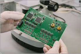
Can printed board assembly be used in high-speed data transmission?
Originally, electronics were assembled using wires connected to each component’s lead. The leads would then be inserted into holes on the copper PCB traces and dip-soldered. However, this was a very tedious and error-prone process. The number of wires involved was also extremely difficult to manage, and the quality of the connections could suffer.
Modern PCBs use a much more efficient and reliable method called surface-mount technology, or SMT, to assemble components. SMT uses automated machines to place components onto the PCB, rather than having a worker hand-insert each component. This saves time and labor, and it reduces human error. In addition, it allows for greater component density on the board.
Before a board can be assembled, it must have a bill of materials (BOM) and Gerber data. A BOM is a complete list of all the required components for the job, including part numbers, quantities, and reference designators. It also includes a column for ‘DO NOT POPULATE’, which is useful for keeping track of all the parts that shouldn’t be installed on the PCB. It’s also helpful for keeping track of the overall assembly costs for each order.
Once the BOM and Gerber files are ready, the board moves on to an inspection process. Depending on the inspection technique, this can be as simple as a 3D solder paste inspection (SPI) or an automated optical inspection (AOI).
A jiggling component or dangling coil can have a huge impact on a device’s functionality, so it’s important to verify that every single component was placed correctly on the board. AOI techniques, for instance, employ autonomous cameras to scan the board and detect errors like solder bridges or missing parts. By incorporating these advanced inspections into the assembly process, manufacturers can improve the reliability of their devices.