solder mask in Pcb assembly companies
Solder mask, also known as solder resist, plays a crucial role in the PCB assembly process, serving as a protective layer that shields the underlying circuitry from environmental factors and prevents solder bridges during soldering. While seemingly inconspicuous, solder mask is a critical component that directly impacts the reliability, functionality, and longevity of electronic devices manufactured by PCB assembly companies.
One of the primary functions of solder mask is to prevent solder bridges or shorts between adjacent copper traces on the PCB. Without solder mask, molten solder could flow freely along the surface of the PCB during the soldering process, leading to unintended connections between conductive traces. These solder bridges can cause electrical shorts, rendering the circuitry non-functional or even damaging components. Solder mask acts as a barrier, covering exposed copper traces and ensuring that solder adheres only to designated areas during soldering, thus preventing shorts and ensuring the integrity of the circuit.
Additionally, solder mask provides protection against environmental factors such as moisture, dust, and chemical contaminants. Exposed copper traces are susceptible to oxidation, which can degrade electrical performance over time. Solder mask forms a protective barrier over the copper traces, shielding them from oxidation and corrosion, and preserving their conductivity and reliability. This protection is particularly important in harsh operating environments or applications where the PCB may be exposed to moisture, humidity, or chemical pollutants.
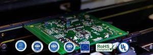
Can you explain the importance of solder mask in Pcb assembly companies?
Furthermore, solder mask enhances the manufacturability of pcb assembly companies by facilitating automated assembly processes. During surface mount technology (SMT) assembly, components are mounted onto the surface of the PCB using solder paste, which is then reflowed to create solder joints. Solder mask helps to define the areas where solder paste should be applied, preventing solder from spreading beyond the intended locations and ensuring precise component placement. This is especially critical for high-density PCBs with closely spaced components, where precise alignment is essential for proper functionality.
Moreover, solder mask aids in the identification and troubleshooting of PCBs during assembly and testing. The contrasting color of solder mask against the underlying PCB substrate provides visual clarity, making it easier for technicians to inspect the board for defects, such as missing components, misaligned solder joints, or solder bridges. By enhancing visibility and facilitating quick visual inspection, solder mask helps to identify and rectify issues early in the manufacturing process, reducing rework and minimizing production delays.
In addition to its functional benefits, solder mask also contributes to the aesthetics of the final product. PCBs with solder mask not only look more professional and visually appealing but also convey a sense of quality and reliability to end-users. Solder mask is available in a variety of colors, allowing PCB assembly companies to customize the appearance of their products to meet specific design requirements or brand preferences.
In conclusion, solder mask plays a multifaceted role in the PCB assembly process, offering protection, functionality, and aesthetic benefits that are essential for producing high-quality electronic devices. By preventing solder bridges, protecting against environmental factors, facilitating automated assembly, aiding in troubleshooting, and enhancing visual appeal, solder mask ensures the reliability, performance, and longevity of PCBs manufactured by PCB assembly companies. As such, solder mask remains an indispensable component in the production of modern electronic devices, enabling the continued advancement and innovation of technology across various industries.